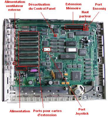
Vous trouverez ci-dessous le brochage de l'ensemble des connecteurs internes de l'Apple IIGS (la carte mère présentée est une ROM03).
| N° de Broche |
Signal |
Description |
| 1 |
GND |
Power and signal ground |
| 2 |
+5V |
+5 volts |
| 3 |
FRA9 |
Ram address bit 9 |
| 4 |
FRA8 |
Ram address bit 8 |
| 5 |
D2 |
Bit 2 of bidirectional data-microprocesseur data bus |
|
| 6 |
FRA6 |
Ram address bit 6 |
| 7 |
FRA3 |
Ram address bit 3 |
| 8 |
FRA4 |
Ram address bit 4 |
| 9 |
FRA5 |
Ram address bit 5 |
| 10 |
FRA7 |
Ram address bit 7 |
| 11 |
+5V |
+5 volts |
| 12 |
FR/W |
Write enable to RAMs ; R/W from microprocessor or DMA |
| 13 |
FRAO |
Ram address bit 0 |
| 14 |
FRA2 |
Ram address bit 2 |
| 15 |
FRA1 |
Ram address bit 1 |
| 16 |
D7 |
Bit 7 of bidirectional data-microprocesseur data bus |
|
| 17 |
/CCAS |
RAM column address strobe |
| 18 |
CROW0 |
Bit 0 for selection of four RAM rows |
|
| 19 |
CROW1 |
Bit 1 for selection of four RAM rows |
|
| 20 |
/CROMSEL |
Card ROM select |
| 21 |
+5V |
+5 volts |
| 22 |
GND |
Power and signal ground |
| 23 |
GND |
Power and signal ground |
| 24 |
+5V |
+5 volts |
| 25 |
D0 |
Bit 0 of bidirectional data-microprocesseur data bus |
|
| 26 |
/CSEL |
Card data buffer direction control |
| 27 |
MSIZE |
Output from card ; indicates RAM row size |
| 28 |
D6 |
Bit 6 of bidirectional data-microprocesseur data bus |
|
| 29 |
D4 |
Bit 4 of bidirectional data-microprocesseur data bus |
|
| 30 |
D5 |
Bit 5 of bidirectional data-microprocesseur data bus |
|
| 31 |
02CLK |
Microprocessor clock |
|
| 32 |
ABORT |
Connect to 65C816 ABORT pin |
|
| 33 |
D3 |
Bit 3 of bidirectional data-microprocesseur data bus |
|
| 34 |
GND |
Power and signal ground |
| 35 |
CRAS |
RAM row address strobe |
| 36 |
D1 |
Bit 1 of bidirectional data-microprocesseur data bus |
|
| 37 |
A10 |
Bit 0 of high-order address bits ; used to decode ROM address |
|
| 38 |
A11 |
Bit 1 of high-order address bits ; used to decode ROM address |
|
| 39 |
A12 |
Bit 2 of high-order address bits ; used to decode ROM address |
|
| 40 |
A13 |
Bit 3 of high-order address bits ; used to decode ROM address |
|
| 41 |
A14 |
Bit 4 of high-order address bits ; used to decode ROM address |
|
| 42 |
A15 |
Bit 5 of high-order address bits ; used to decode ROM address |
|
| 43 |
+5V |
+5 volts |
| 44 |
GND |
Power and signal ground |
| N° de Broche |
Signal |
Description |
| 1 |
/IOSEL |
Input/Output Selection (driven by the 65C816) |
| 2 |
A0 |
Bit 0 of the three-state address bus |
| 3 |
A1 |
Bit 1 of the three-state address bus |
| 4 |
A2 |
Bit 2 of the three-state address bus |
| 5 |
A3 |
Bit 3 of the three-state address bus |
| 6 |
A4 |
Bit 4 of the three-state address bus |
| 7 |
A5 |
Bit 5 of the three-state address bus |
| 8 |
A6 |
Bit 6 of the three-state address bus |
| 9 |
A7 |
Bit 7 of the three-state address bus |
| 10 |
A8 |
Bit 8 of the three-state address bus |
| 11 |
A9 |
Bit 9 of the three-state address bus |
| 12 |
A10 |
Bit 10 of the three-state address bus |
| 13 |
A11 |
Bit 11 of the three-state address bus |
| 14 |
A12 |
Bit 12 of the three-state address bus |
| 15 |
A13 |
Bit 13 of the three-state address bus |
| 16 |
A14 |
Bit 14 of the three-state address bus |
| 17 |
A15 |
Bit 15 of the three-state address bus |
| 18 |
A2R/W |
Three-State read/write line |
| 19 |
/SYNC |
Composite horizontal and vertical sync (only for slot 7 ; no connextion on the other 6 slots) |
| 20 |
/IOSTRB |
Goes low when the 65C816 adresses a location between $C800 and $CFFF |
|
| 21 |
RDY |
Input to the 65C816 |
| 22 |
/DMA |
Input to the address bus buffer |
| 23 |
INT OUT |
Interrupt priority daisy-chain output (no connection for this pin on slot 7) |
| 24 |
DMA OUT |
DMA priority daisy-chain input (no connection for this pin on slot 7) |
| 25 |
+5V |
+ 5 volt power supply |
| 26 |
GND |
System common ground |
| 27 |
DMA IN |
DMA priority daisy-chain input (on slot 1 only, this pin has no connection) |
| 28 |
INT IN |
Interrupt priority daisy-chain input (on slot 1 only, this pin has no connection) |
| 29 |
/NMI |
Nonmaskable interrupt to 65C816 |
| 30 |
/IRQ |
Interrupt request to 65C816 |
| 31 |
/RST |
Reset routine |
| 32 |
/INH |
Disable memory on the main circuit board |
| 33 |
-12V |
- 12 volt power supply |
| 34 |
-5V |
- 5 volt power supply |
| 35 |
CRF |
3.58 MHz color-reference signal (for slot 7 only) |
| 35 |
M2B0 |
Mega II bank 0 signal (256K Apple IIGS : slot 3 only - 1 MB Apple IIGS : slot 1-6) |
| 36 |
7M |
System 7 MHz clock |
| 37 |
Q3 |
System 2 MHz asymmetrical clock |
| 38 |
01 |
01 clock |
| 39 |
/M2SEL |
The Mega II select signal |
| 40 |
00 |
00 clock |
| 41 |
/DEVSEL |
Goes low during 00 when the 65C816 adresses location $C0nx |
| 43 |
D7 |
Bit 7 of three-state buffered bidirectional data bus |
| 44 |
D6 |
Bit 6 of three-state buffered bidirectional data bus |
| 44 |
D5 |
Bit 5 of three-state buffered bidirectional data bus |
| 45 |
D4 |
Bit 4 of three-state buffered bidirectional data bus |
| 46 |
D3 |
Bit 3 of three-state buffered bidirectional data bus |
| 47 |
D2 |
Bit 2 of three-state buffered bidirectional data bus |
| 48 |
D1 |
Bit 1 of three-state buffered bidirectional data bus |
| 49 |
D0 |
Bit 0 of three-state buffered bidirectional data bus |
| 50 |
+12V |
+ 12 volt power supply |